 ©2023 Yann Guidon
all documentation published under CC BY-NC-SA 4.0 license.
©2023 Yann Guidon
all documentation published under CC BY-NC-SA 4.0 license.
Created sam. 30 sept. 2023 21:52:48 CEST by whygee@f-cpu.org Version sam. 16 déc. 2023 05:22:02 CET PRELIMINARY / WORK IN PROGRESS It's not yet a reliable and definitive reference! Check the latest news and updates at ygrec8.com and download the latest version from src.ygrec8.com or if you prefer git : gitlab.com/fhwd/ygrec8
Along with this document, you should also read:
This manual describes one intended implementation for integration in a microchip. Other structures and organisations might be used for other technologies.
A complete and functional YGREC8 system requires more than the main datapath. The following diagram shows the other necessary blocks :

The debug system is essential during development: this is the circuit that lets the developer write and read data inside the system. It can access:
The clocks are very different so the commands are resynchronised by talking to the FSM, which also receive a small set of commands such as RESET, START, STEP, STOP, WR_INSTR, WR_IMEM etc. The FSM can also inhibit the update of the registers or the PC for example, so the currently injected instruction is not considered as coming from the program memory's instructions stream.
From there, the developer can inject arbitrary instructions to access the other parts of the system (memory blocks, I/O etc.), dump or modify the state of the system... The debug circuits are totally asynchronous from the main clock, and usually significantly slower. The developer must stop the core when inspecting or writing data. It is a bit more intrusive than other debug systems but it is designed to use as few transistors as possible.
A version of the debug circuit called DTAP has already been designed as a standalone circuit but it could be replaced by anything that does the job, such as the Caravel harness used by eFabless (though it is much more complex and uses more real estate, meaning it is more prone to failure). Or a more classic JTAG scan chain.
The core should be able to work in "standalone" mode, when no host controls the debug circuits. This is usually controlled by the state of some pins during /RESET : the System FSM can wait for a debugger to take control, or the FSM can load external instructions, either passively (as a SPI slave) or actively (by reading from an external SPI Flash chip). If the Y8 system has no internal code storage, you can bootstrap the core by sending 512 bytes through SPI (with an Arduino, RPi or ESP). The System FSM also handles the RESET/LOAD/START/STEP/SKIP/STOP commands received from the debugger.
The Instruction FSM manages the lower-level details of scheduling the instructions and their details (such as OVL, HLT, LDCx, writes to PC...). This split of the FSM greatly simplifies the design and the modularity. More states are added as more features and corner cases are developed. Meanwhile, the System FSM remains core-agnostic.
The Y8 core does most of the remaining work : decodes instructions, fetches operands, performs operations, writes the results to the registers, checks conditions and move things around... It reads instructions from the Instruction Register, which usually transparently interfaces the Instruction SRAM. The instruction can also be read or written by the debug circuit, for inspection, injection as well as for writing a new program or overlay into the Instruction SRAM.
The Data SRAM is just a plain memory array. 2 areas of 256 bytes each do the trick but some banking could take place if needed and if the necessary resources are available.
The IO & Config Registers is a user-defined area of 512 bytes that does
everything that the rest can't. This is usually where customisation takes place, signals
enter or exit the system, default behaviours are configured...
Still missing : the interrupt controller and exception handling (everything jumps back
to address 0 for now). Stay tuned.
The default implementation of the debug system is the DTAP, which is now spun off into a parallel project. A simulator or emulator can easily perform its function during development.
The interface between the debug circuit is asynchronous, must be correctly sampled (beware during signal transitions) and the rest of the Y8 system must have at least these signals :
and probably more but not much because most basic functions are already possible with some combination of commands.
The System FSM is part of the Y8 system, it is clocked like the core and helps synchronise the debug commands. It manages initialisation, loads the initial code overlay, controls the high-level core behaviour and interfaces with the debug system. See this discussion.
The host controls the debug session and is responsible for enforcing correct sequences and timing to prevent overlaps or undefined states. Going from one state to another must use a buffer NOP command. Some states are duplicated to allow the command register to contain single-cycle orders during multiple cycles (STEP, SKIP, WR_IMEM...). Four states are reached when the command goes back to NOP. Here is a (preliminary) list of the commands that the System FSM can receive:
The internal states can be read by the debug system.

Some of the required inputs for this FSM:
Some of the required outputs for this FSM:
This is the ISA-specific part of the scheduling system, which needs more direct information from the core, in particular from the instruction decoder.
The PRFX state is almost identical to the INST state, with some transition conditions to IDLE inhibited (RUN, STEP...).

BTW it would be extra cringe to have an instruction sequence like PF PC , LDCH R1 R1 or something like that, since it would scan several different states in sequence, for no useful purpose. But the FSM must not let such a corner case fall into a crack...
Some of the required inputs for this FSM:
Some of the required outputs for this FSM:
This FSM will stop if the instruction is not a valid one, if more than one prefix is used or if an overlay is requested. The System FSM will manage what to do with these conditions: reboot ? load or switch to a different overlay ? This is discussed later in this manual but so far, the core reboots or freezes.
At the start, it is a simple latch to buffer the Instruction Memory's output. The memory's read port is also multiplexed with another register written by the debug system to inject arbitrary instructions.
The program memory is directly addressed by the PC register (to prevent circuit duplication). During an overlay load sequence (controlled by the System FSM), the PC is reset then incremented, all core WriteBacks are inhibited, the Instruction Register is loaded with new values then it is written to the instruction memory. The cycle stops when the PC has overflown, reaching again a cleared state, and execution resumes.
More features can be added to this simple unit, to allow better debugging by triggerring traps and/or incrementing event counters:
The instruction register could also later inject one or more prerecorded instruction sequences to manage transitions (such as state backup/restoration) when an exception or IRQ occurs, so a small SRAM or ROM block might emulate microcode (as a last resort because the FSMs must also be adapted).
...
The core's speed should be decent, with a pretty short critical datapath, and most of the instructions execute in one clock cycle. Exceptions include the LDCx instructions, computed writes to PC and prefixes.

Legend:
The exceptions and scheduling are handled by the System FSM and the Instruction FSM.
Memory blocks expect a stable address to be latched at the start of every clock cycle. Both Program Memory and Data Memory operate simultaneously, independently, they are not multiplexed.
The Data Memory could be a single SRAM block because only one register can be updated during a cycle. A1, D1, A2 and D2 can act as "cache" for the memory blocks. The single-memory-block case adds some complexity because A1 and A2 must be multiplexed for each access. Using two independent blocks looks easier at first because their respective addresses are taken directly from A1 and A2.
The program memory is a bit more delicate because the incremented address from PC must first be latched. Depending on the latency ratio between the memory and the core, there are two possible configurations:
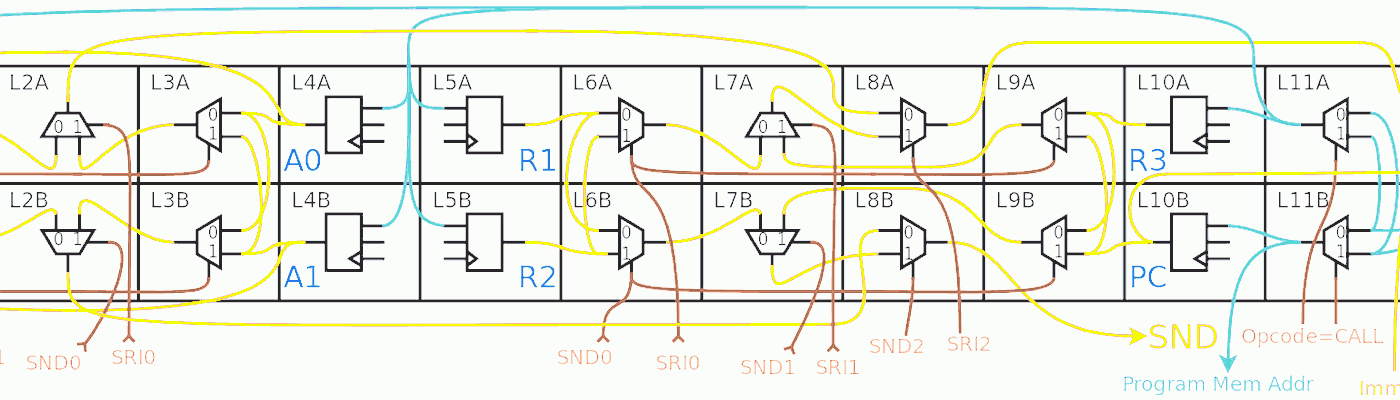
The datapath is conceptually split into 2 stages:
The first stage is typically as fast as the increment of the PC so the value of SRI can be multiplexed directly to the Instruction Memory address bus. This allows some operations like LDCx, CALL or SET to execute with no stall. However if the value must pass through the other units, such as during a relative jump (or any other "write to PC" instruction), the instruction fetch is stalled while waiting for the result to be available on the Suxen hub. This is why the Instruction FSM has an extra "write to PC" stall state. Of course, this is only a suggested organisation and the scheduling can be widly different in other situations.
The 512 registers are only accessed with an immediate address to shorten the decoding time and give enough time for the many registers to react. This bus has a very large fan-in and fan-out, on top of the complex decoding, so it is expected to be "slow". Eventually, wait states could be added in the FSM if the IO bus is too crowded.
The IO system is modular, user-defined, so it is not part of the core. Indirect addresses might be possible (and even self-incrementing) through specific registers but this is independent from the core as well. There is a simple synchronous interface, without indication that the address is implemented (or not):
There is no standard map of the IO space, but here are some of the intended uses :
As already mentioned, fan-in and fan-out is the main challenge. The addresse maps change wildly across implementations because decoding can use boolean shortcuts. This is also why 9 bits are used, and not 8 : some address bits could be directly used as "enable" signals. This is discussed here but too many things have changed since. The interface names should be standardised to allow porting the source code, and the address map could be "compiled" with some smart software (one day).
The YGREC8 has a lousy addressing space, like we're in 1972 or so. There is no split of the addressing space into several remapped banks like in other 8-bit CPUs (Z80 or 68xx). The approach is to simply swap or switch the whole program memory to different contents. In the YGREC8 system, each block of 256 instructions is called an overlay.
A program can switch to a different overlay by hijacking the CALL instruction: it makes no sense to CALL and write the PC+1 to PC so this is interpreted as the OVL opcode. The operand can be a register, a 4-bit or 8-bit immediate, and the first operands allow conditions. Since a register can be an operand, it is possible for an overlay to "call" another, which can then "return" to the first one when a function is completed. Saving the PC+1 adds some overhead though.
Overlays can later be used to handle traps, interrupts and other system management tasks, and the YGREC8 could cycle through several "user" overlays, which share common functions provided by yet other "library" overlays.
How many overlays can there be ? Maximum 256 since the OVL opcode can only specify one byte. The value 255 means HALT and is currently hardwired to stop the core (it may be implemented as a real overlay that provides some debug functions). Overlay#0 is the bootstrap overlay. Overall, the 64Ki instructions (128KiB) could look like this:
So far, exceptional conditions are not handled specifically and it causes the System FSM to reboot the core. A "reason" I/O register would help distinguish the sources of reboot but with a space of only 256 instructions, there is not much to both do and catch.
A larger program memory space will help with easier handling: the traps and interrupts can then be configured to switch to a user-given overlay.
To be continued...